


Factory Direct Pricing | Bulk Orders Available
The conductive patterned coating based products are one of the most in-demand products in numerous industries today. There are multiple industrial, commercial, and optoelectronic applications for patterned conductive glass. Our products continue to be extraordinarily environmental and temperature-friendly thanks to their higher level of stability.
The conductive patterned coating manufactured by us provides excessively low resistance, thanks to the extremely low pinhole density of our advanced and innovative ion-assisted electron beam sputtering method which used for coating. It, in turn, allows our coatings to be remarkably low defect coatings.
The excellent quality of material and ultra-modern coating technique allows the patterned conductive glass to use in the highest and lowest of temperature, with equal efficiency. Our ITO coated patterned PET is of extremely high-quality and gets a full-surface coat of ITO (Indium Tin Oxide), making it remarkably conductive to electricity. Not only this, but the FTO coating also leaves the substrate with higher optical transmission power.
As per customer’s requirement, we are also fully capable of supplying glass/plastic substrates coated with layers other than ITO, such as dielectric layers for index matching, or anti-reflective purposes.
The conductive patterned coatings produced by us are completely high-quality and effective. These properties make our ITO coated patterned glass an excellent product for numerous industries and R&D institutes:
| Conductive Patterned Coating – Technical Specifications | |
|---|---|
| Coating Thickness | 200 nm – 30 microns |
| Coating Materials | ITO, FTO, AZO, Mo |
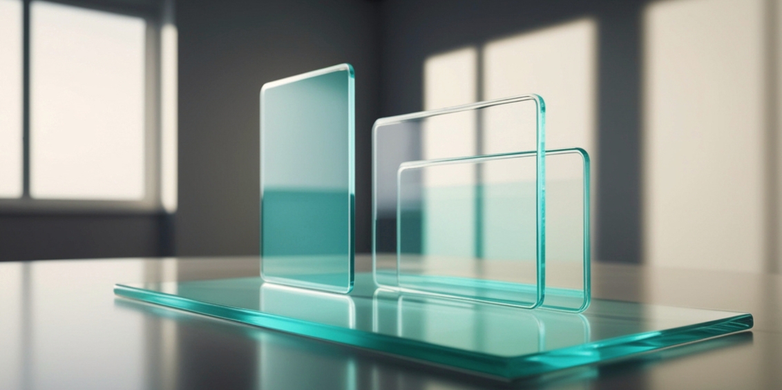
| Appearance | Highly transparent colored glass / plastic substrate |
| Substrate Thickness | 0.5 mm – 1.1 mm |
| Specific Weight | ~8 kg/m² (for 3.2 mm / 1/8” glass) |
| Transmittance | > 83% – > 87% |
| Light Spectrum Range | Infrared to Ultraviolet |
| Coating Method | Chemical / Laser Etching |
| Substrate Size | Length: 950 mm – 2150 mm Width: 650 mm – 1220 mm (Custom sizes available) |
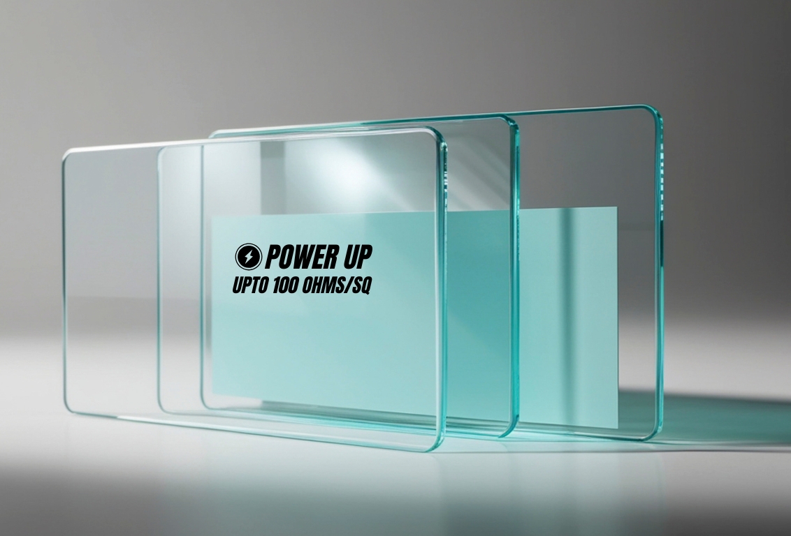
| Sheet Resistance | 10 – 100 ohms/sq (standard) |
| Temperature Resistance | Up to 500°C (beyond this glass may melt) |
| Mechanical Strength | 90 MPa |
| Poisson Ratio | 0.2 |
| Density | 2500 kg/m³ |
| Property | ITO Coating | FTO Coating | AZO Coating | Mo Coating |
|---|---|---|---|---|
| Full Form | Indium Tin Oxide | Fluorine-doped Tin Oxide | Aluminum-doped Zinc Oxide | Molybdenum |
| Transparency | Very High (>85%) | High (>80%) | High (>80%) | Low (Opaque) |
| Conductivity | Excellent | Very Good | Good | Excellent |
| Sheet Resistance | 10 – 100 Ω/sq | 10 – 15 Ω/sq | 20 – 200 Ω/sq | < 5 Ω/sq |
| Cost | High | Moderate | Low | Moderate |
| Thermal Stability | Moderate | Excellent (High Temp Stable) | Good | Excellent |
| Chemical Stability | Moderate | Excellent | Good | Excellent |
| Flexibility | Low | Low | Better than ITO | Low |
| Typical Applications | Touchscreens, Displays, Solar Cells | Solar Cells, Heated Glass | Solar Cells, Displays (Cost-sensitive) | Back Contacts, Electrodes |
| Patterning Compatibility | Excellent (Laser/Chemical) | Good | Good | Excellent |
Expert’s advice to handle our FTO coated patterned glass products with care when transporting or storage. Ensure that the product is stored at average room temperatures and cleaned thoroughly before being used. Never use the product in applications which exceed 500˚ C, as it risks the substrate being melted at such high temperatures.
We are a notable manufacturer and supplier of patterned conductive glass in India, Asia, EU, and other parts of the globe. The brand is synonymous with designing and providing excellent-quality conductive patterned coating based products, in standard dimensions as well as customized type, size, and shape, all precisely according to individual client’s requirements.